The wiring diagram illustration - the breadboard is opposite the from the photo of the finished . I matching the wiring of the illustration - wrecked my board and ADCO0834. Can you confirm which diagram should be followed - as the baord would be reverees that would of course switch grounding pins to the hot so what happened
— meaning Pin 5 is getting 5V and Pin 10 is getting GND — the chip will draw excess current internally, often from VCC to GND → this causes the chip to heat up and melt the breadboard plastic underneath. Please advise
Please follow the wiring diagram for correct connections (as shown in the picture).
For the ADC0834 module:
- Insert it into the breadboard in the correct orientation (with the lettering facing upright).
Additionally:
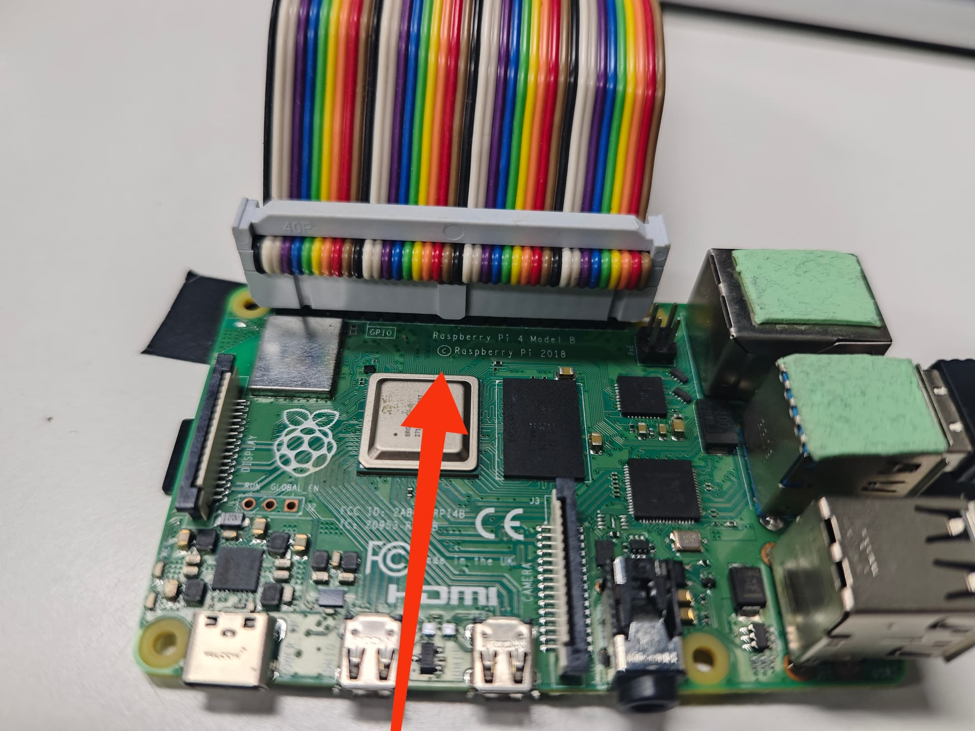
- How did you connect the ribbon cable between the Pi and the T-connector?
- Please refer to our provided reference images for proper connection.


Why are the images at the end - the photos all incorrect ? what are there purpose 2. I followed the purposed wiring diagram and had my ADC0834 in the correct position and it still melted my board. You are sure the Breadboard position faces 60-1 and not 1-60?
Also even in your photo and the schematic - the schematic shows dead center but yours is off becuase it has to be bas on the odd spacing. How did you know to move the GPIO baord closer to the top and now the bottom? The board is at 40 but not covering 40 , but the schematic shows its covering 40 partially but mine is not covering 40 at all yet all pins are in
Please share your wiring diagram with us.
Note:
- For breadboard connections, wiring from 60→1 or 1→60 both work fine
- You can simply follow the standard wiring diagram for installation
Regarding your ADC0834 module:
- Has it burned out?
- Are there any other damaged components?
Please provide photos of the issue to help us better assist you.